Tech Stack
Our Technology Foundation
Vayuvyastra Semicon leverages cutting-edge semiconductor technologies and industry-standard tools to deliver world-class solutions. Our technology foundation spans advanced process nodes, modern design methodologies, and comprehensive EDA tool expertise.
We continuously invest in R&D to stay at the forefront of semiconductor innovation, ensuring our solutions meet the evolving demands of modern applications.
Process Technology Insights
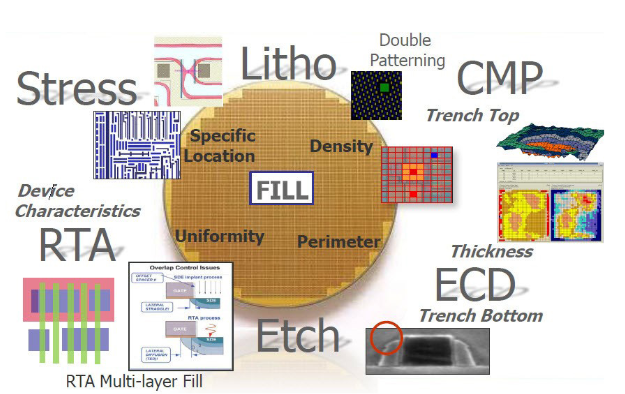
Deep understanding of CMOS, FinFET, and GaN processes
Industry-Grade EDA Tools
Expertise across leading EDA platforms and flows